RISC-V & Rust 3: Initializing DRAM and clocks
Table of contents
- 1. Introduction
- 2. System bus tree overview
- 3. Initializing clocks
- 4. Initializing DRAM controller
- 5. What's next?
1. Introduction
Up until now, we were basically exploring the hardware platform and setting things up without following any particular direction. Let's fix that.
Here's a concept of a plan (tee hee) of the future work:
Part I: bootloader (you are here). If we're ever going to make an OS, we'll need to build a bootloader for it first. We're actually half way there -- almost -- as the only missing pieces are DRAM and CCU (clock controller unit) initialization and kernel image loading code. These will be the focus of this and the following articles.
Part II: kernel (maybe several articles later). Here we'll start working on the OS kernel. The key tasks will include: setting up timer interrupts, initializing virtual memory, implementing kernel threads and context switching, implementing userland processes and syscalls.
Part III: userland (distant future). We will need to setup boot process (init RAM disk), a file system, some system services and basic drivers. After that, possibilities are endless. We can write our own command shell, maybe some basic POSIX compatibility layer so we can cross compile parts of coreutils, GUI.. ugh
Now, let's wake up to the cruel real world where our biggest achievement is UART hello world, and get back to work. In this article we will be initializing peripherals clocks and the DRAM controller, which will get us ready for booting the kernel.
2. System bus tree overview
Before we start writing code, let's take a deeper dive into the variety of SoC buses and peripherals so that we have at least basic understanding on what we're doing and not just blindly rewrite the sunxi SPL code.
Here are a couple of diagrams from D1 User manual that can help us.
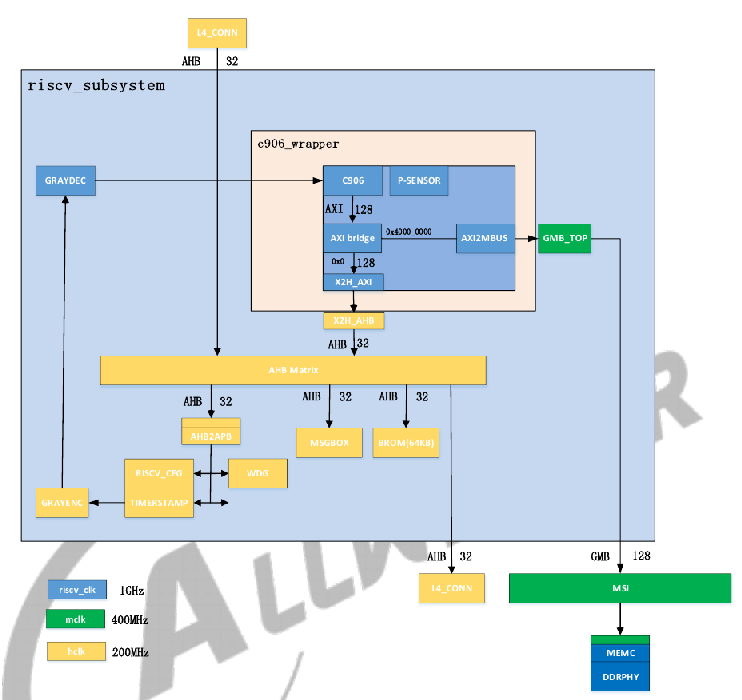 RISC-V System Block Diagram (figure 3-9 from D1 User Manual V1.0)
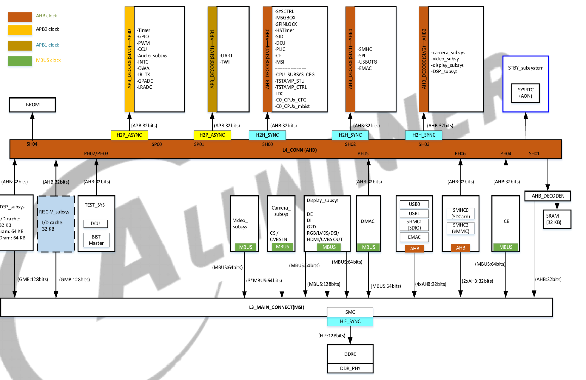 System bus tree (figure 3-2 from D1 User Manual V1.0)
From these diagrams we can see that RISC-V core (C906) uses AXI bus to connect to the outside world. High speed peripherals (e.g. SMHC/USB/SPI/MSGBOX) are connected to AHB interface, which is in turn connected to AXI bridge. Low speed peripherals (e.g. UART, GPIO, timers) are connected to two APB buses (one for UART and TWI, and the other for others). AXI, AHB and APB are a part of well-established open standard for on-chip interconnect interfaces called AMBA (Advanced Microcontroller Bus Architecture) developed by Arm.
The memory controller (MEMC/DDRPHY) is connected to the RISC-V core using MSI (Memory System Interface ?) bus. All DMA-capable peripherals are connected to MSI (MBUS) too so that they can talk to the memory controller. I couldn't find any information about this MSI/MBUS interface in the docs or on the internet so let's just accept its existence and move on. I couldn't find any info about the memory controller either, but more on that later.
There are two more diagrams in the "3.2 Clock Controller Unit" section (Module Clock Generation and PLL distribution) that are worth checking out. Personally I've found those more confusing than helping, though. Another good source of information here is the linux kernel (see source/drivers/clk/sunxi-ng/ccu-sun20i-d1.c) and sunxi SPL (as always). Sadly, u-boot is almost useless here, as seem to be only setting up the CPU PLL, delegating the rest to the linux kernel.
There are difficulties with using both linux kernel and sunxi SPL as a reference, as kernel's sunxi clk driver is heavily abstracted, so you have to go through layers and layers of macros to get down to the register level. And sunxi SPL seems to be doing some straight up weird stuff, and didn't even initializing some things (although I am not really sure those were really necessary).
We also need to figure out clock rates for each bus. The only thing we known from the SBC docs is that the CPU is running at 1GHz, so we have to refer to sun20i SPL sources or Linux kernel to get more information. The SPL clocks setup code (see board/sun20iw1p1/clock.c) is pretty straightforward, but I decided to cross check with the linux kernel, as it has some weird things here and there.
Figuring out actual clock rates in linux just from the source code may be quite complicated process because of how bottom up clock rate propagation works, so it is easier to just look it up in runtime. The clock tree is easily available via debugfs: cat /sys/kernel/debug/clk/clk_summary. This will print a nicely formatted representation of all clock in the system:
                                 enable  prepare  protect                                duty  hardware
   clock                          count    count    count        rate   accuracy phase  cycle    enable
-------------------------------------------------------------------------------------------------------
 dcxo                                10       10        0    24000000          0     0  50000         Y
    osc24M-32k                        0        0        0       32000          0     0  50000         N
    apb1                              1        1        0    24000000          0     0  50000         Y
       bus-uart0                      1        1        0    24000000          0     0  50000         Y
    cpux                              1        1        0    24000000          0     0  50000         Y
       cpux-apb                       0        0        0     6000000          0     0  50000         Y
       cpux-axi                       0        0        0    24000000          0     0  50000         Y
    pll-periph0-4x                    1        1        0  2400000000          0     0  50000         Y
       pll-periph0-800M               0        0        0   800000000          0     0  50000         Y
       pll-periph0-2x                 2        2        0  1200000000          0     0  50000         Y
          fanout-32k                  0        0        0       32768          0     0  50000         N
             fanout2                  0        0        0       32768          0     0  50000         N
             fanout1                  0        0        0       32768          0     0  50000         N
             fanout0                  0        0        0       32768          0     0  50000         N
          pll-periph0-div3            0        0        0   200000000          0     0  50000         Y
          pll-periph0                 4        4        0   600000000          0     0  50000         Y
             mmc1                    21       21        0    50000000          0     0  50000         Y
             mmc0                     0        0        0    50000000          0     0  50000         N
... truncated
Putting all the pieces together we get the following summary.
| BUS/PLL/Module | Clock rate | Clock Source |
|---|---|---|
| CPU PLL | 1008 MHz | DXCO (24 MHz) |
| RISC-V core | 1008 MHz | CPU PLL |
| RISC-V AXI | 504 MHz | CPU PLL |
| Peripheral PLL 1x | 600 MHz | DXCO |
| AHB | 200 MHz | Peripheral PLL 1x |
| APB0 | 100 MHz | AHB |
| APB1 | 24 MHz | DXCO |
3. Initializing clocks
Now we can finally put our hands on the code. We'll steal most of it from the sunxi SPL, as at this stage we just want to get it working and move on to working on the kernel. We can revisit it when we'll start working on drivers.
3.1 CPU PLL
We'll initialize the CPU PLL first. We'll need to do the following:
- Temporarily switch the CPU core to some other clock source (e.g. DXCO) so we can configure the PLL.
- Disable the clock signal from the PLL (gating) and set the factor. PLL clock rate formula is
24 MHz * N / M. To get the desired rate of 1008 MHz, we need to set N to 24 and M to 1. - Start PLL lock and wait for it to become stable.
- Enable PLL clock signal.
Here's the code that does this:
// Temporarily reparent RISC core clock to 24MHz HOSC while we're setting up the PLL
Reg32::zero(CCU_BASE + CCU_RISCV_CLK)
    .set_field::<24, 2>(0) // RISC-V_CLK_SEL = HOSC (0)
    .set_field::<8, 2>(3) // RISC-V_AXI_DIV_CFG (Factor N) = 3
    .set_field::<0, 1>(1) // RISC-V_DIV_CFG (Factor M) = 1
    .write();

udelay(1);

// Disable gating
Reg32::read(CCU_BASE + CCU_PLL_CPU_CTRL)
    .set_field::<27, 1>(0) // PLL_OUTPUT_GATE = 0
    .write();
Reg32::read(CCU_BASE + CCU_PLL_CPU_CTRL)
    .set_field::<30, 1>(1) // PLL_LDO_EN = 1
    .write();

udelay(5);

// PLL freq = 24MHz * N / M  = 24 * 42 / 1 = 1008 Mhz ~ 1GHz
Reg32::read(CCU_BASE + CCU_PLL_CPU_CTRL)
    .set_field::<8, 8>(41) // PLL_N = 41
    .set_field::<0, 2>(0) // PLL_M = 0
    .write();

// Enable PLL lock
Reg32::read(CCU_BASE + CCU_PLL_CPU_CTRL)
    .set_field::<29, 1>(1)
    .write();

// Enable PLL
Reg32::read(CCU_BASE + CCU_PLL_CPU_CTRL)
    .set_field::<31, 1>(1)
    .write();

// Wait for PLL lock to become stable
Reg32::read(CCU_BASE + CCU_PLL_CPU_CTRL).wait_bit::<28>(true);
udelay(20);

// Disable gating
Reg32::read(CCU_BASE + CCU_PLL_CPU_CTRL)
    .set_field::<27, 1>(1)
    .write();

// Disable PLL lock
Reg32::read(CCU_BASE + CCU_PLL_CPU_CTRL)
    .set_field::<29, 1>(0)
    .write();

udelay(1);

// PLL is ready to use
3.2 RISC-V core and AXI
Next, we'll initialize the CPU clock. Initialization steps are:
- set CPU clock source back to CPU PLL
- set the CPU clock divisor to 1, as we want it to run at 1GHz too
- set AXI clock divisor to 2 so it runs at 500 Mhz.
One interesting thing is that there seems to be two registers related to the AXI and CPUX clocks: CCU_CPU_AXI_CFG (0x500) and CCU_RISCV_CLK (0xD00). Both have clock source fields and AXI clock div factor. SPL only uses the latter. Linux kernel has definitions for both in the clock tree, but the former seems to be left unset (set to DXCO as a clock source). I suspect that CCU_CPU_AXI_CFG is an leftover from ARM SoCs, as the whole CCU module seems to be reused by Allwinner from their ARM based processors.
// - Reparent RISCV core clock to CPU PLL
// - RISCV core clock freq = PLL_CPU / M = 1008 MHz ~ 1 GHz
// - RISCV AXI freq = PLL_CPU / N = 504 MHz
Reg32::read(CCU_BASE + CCU_RISCV_CLK)
    .set_field::<0, 4>(0) // RISC-V_DIV_CFG (factor M - 1) = 0
    .set_field::<8, 2>(1) // RISC-V_AXI_DIV_CFG (factor N - 1) = 1
    .set_field::<24, 3>(5) // RISC-V_CLK_SEL = PLL_CPU
    .write();

udelay(1);
Now the CPU should be running at the 1 GHz. Yay.
3.3 PERI PLL, AHB and APB0
All three peripherals PLLs (PERI_PLL 2x @ 1200 MHz, PERI_PLL 1x @ 600 Mhz, PERI_PLL 800MHz) seem to be already up and running after the CPU reset, and the docs strongly advise against changing their default clock rates, so we'll simply skip the initialization. The SPL is effectively doing the same, but checks if they are initialized first, which is in practice always the case.
AHB and APB0 initialization is simple:
// AHB clock = PLL_PERI(1X) / M / N = 200Mhz

Reg32::zero(CCU_BASE + CCU_PSI_CLK)
    .set_field::<0, 2>(2) // FACTOR_M = 0
    .set_field::<8, 2>(0) // FACTOR_N = 0
    .write();

Reg32::read(CCU_BASE + CCU_PSI_CLK)
    .set_field::<24, 2>(3) // CLK_SRC_SEL = PLL_PERI(1X)
    .write();

udelay(1);

// APB0 CLK = PLL_PERI (1x) / M / N = 100Mhz

Reg32::zero(CCU_BASE + CCU_APB0_CLK)
    .set_field::<0, 5>(2) // FACTOR_M = 2
    .set_field::<8, 2>(1) // FACTOR_N = 1
    .write();

Reg32::read(CCU_BASE + CCU_APB0_CLK)
    .set_field::<24, 2>(3) // CLK_SRC_SEL = PLL_PERI(1X)
    .write();

udelay(1);
We'll skip APB1 initialization as the defaults after the reset (24Mhz from the DXCO) seem to be perfectly fine. Both SPL and linux kernel don't change these as well.
3.4 Other stuff
As a part of clock initialization, sun20i SPL also de-asserts the DMA engine and MBUS clocks. MBUS clock is properly initialized later during DRAM controller initialization. I am not sure how necessary is all of this, so I've kept it just in case. I've also added the calculation and printing of the resulting clock rates, so all the relevant clock rates are nicely printed at boot.
I am omitting those things as they are rather uninteresting (see the full sources for the article: source).
4. Initializing DRAM controller
Now, this is where water gets murky. Turns out, there is no publicly available documentation on the DRAM controller. To add to that, it looks like the original DRAM controller initialization code (libdram) had originally been shipped either as a compiled object or assembly source and later was decompiled or rewritten in C. There are quite extensive comments in the decompiled code, but I cannot claim that I understood everything there as my experience with DRAM controllers is limited, so take my explanations below with a grain of salt. Here's a cool introduction to DRAM inner workings: https://www.systemverilog.io/design/ddr4-basics/.
The original DRAM initialization code is a single 1700+ LOC file that is full of magic values written to magic registers and puzzled comments of someone who was reverse engineering all of this. You can find it at drivers/dram/sun20iw1p1/lib-dram/mctl_hal.c in sun20i-spl sources. U-Boot code is almost the same (see drivers/ram/sunxi/dram_sun20i_d1.c), but is a little bit more tidied-up and also has some extra comments.
I didn't really want to spend much time rewriting all of this in proper idiomatic Rust, as I simply wanted to make DRAM work and move on. So I started looking for shortcuts:
The obvious thing to do is to simply link whole
libdramto Rust code and call it a day. This would require a C cross toolchain installed and doesn't feel "clean" enough overall. Meh.libdramcan initialize any DRAM type supported by the controller, but we can cut the amount of code significantly by dumping the configuration specifically for the DRAM chip onboard of MangoPi MQ Pro. This will decrease the amount of code about tenfold, but adapting our bootloader to another D1-based SoC will be a lot of work. Still meh.Automatic code translation. There are tools like
c2rustthat provide automatic C to unsafe Rust code migration. Also, it is 2024, so why not just throw it at an LLM? They are getting quite smart these days, although we'll still have to proofread the output.
Ultimately, I chose the third option. Initially, I reached for c2rust, as old-school algorithmic code translation seemed more robust to me. But results were too true to the original and required a good clean up. Here's an example:
unsafe extern "C" fn mctl_com_init(
    mut para_0: *const dram_para_t,
    mut config: *const dram_config_t,
) {
    let mut val: uint32_t = 0;
    let mut width: uint32_t = 0;
    let mut ptr: libc::c_ulong = 0;
    let mut i: libc::c_int = 0;
    clrsetbits_le32(
        0x3102008 as libc::c_int as uint32_t,
        0x3f00 as libc::c_int as uint32_t,
        0x2000 as libc::c_int as uint32_t,
    );
    val = readl(0x3102000 as libc::c_int as uint64_t)
        & !(0xfff000 as libc::c_int) as uint32_t;
    val |= ((*para_0).dram_type & 0x7 as libc::c_int as uint32_t) << 16 as libc::c_int;
    val |= (!(*config).dram_para2 & 0x1 as libc::c_int as uint32_t) << 12 as libc::c_int;
    val |= BIT(22 as libc::c_int as uint32_t);
    if (*para_0).dram_type == SUNXI_DRAM_TYPE_LPDDR2 as libc::c_int as uint32_t
        || (*para_0).dram_type == SUNXI_DRAM_TYPE_LPDDR3 as libc::c_int as uint32_t
    {
        val |= BIT(19 as libc::c_int as uint32_t);
    } else if (*config).dram_tpr13 & BIT(5 as libc::c_int as uint32_t) != 0 {
        val |= BIT(19 as libc::c_int as uint32_t);
    }
    // truncated..
c2rust includes a tool for rule-based refactoring, which can help further refine the code. However, it is not something you can master in a hour. I probably could have done this manually with a little help of vim macros and regexes, but decided to embrace modernity and give LLMs a chance.
In the end, I've ended up converting most of the code using ChatGPT with 4o model. It was instructed to keep the code as close to the original as possible to make review process easier. It actually did a good job and I only had to change minor syntax flops in macros here and there. Here's the same function translated by the LLM:
unsafe fn mctl_com_init(para: &DRAMParam, config: &DRAMConfig) {
    let mut val: u32;
    let width: u32;
    let mut ptr: u64;
    let mut i: u32;

    // purpose ??
    clrsetbits_le32(0x3102008, 0x3f00, 0x2000);

    // set SDRAM type and word width
    val = readl(0x3102000) & !0x00fff000;
    val |= (para.dram_type & 0x7) << 16; // DRAM type
    val |= (!config.dram_para2 & 0x1) << 12; // DQ width
    val |= bit(22); // ??
    if para.dram_type == SUNXI_DRAM_TYPE_LPDDR2 || para.dram_type == SUNXI_DRAM_TYPE_LPDDR3 {
        val |= bit(19); // type 6 and 7 must use 1T
    } else {
        if (config.dram_tpr13 & bit(5)) > 0 {
            val |= bit(19);
        }
    }
    // truncated..
Again, full code is around 2K LOC, so I won't list it here. Here's a gist of what DRAM initialization code does:
- Impedance (ZQ) calibration (in
do_init_dram). - Setting voltages (
dram_voltage_set). - Determining DRAM topology (
auto_scan_dram_config).- Finding out the number of ranks (a set of DRAM chips sharing single a chip select) and DQ (data bus) width:
auto_scan_dram_rank_width. - Determining DRAM size (
auto_scan_dram_size). This is done by writing a test pattern and then reading it back until the addresses wrap is detected. This way it detects the number of rows, then the number of banks and then the number of columns.
- Finding out the number of ranks (a set of DRAM chips sharing single a chip select) and DQ (data bus) width:
- Final initialization using the parameters found at previous steps.
- Doing some magic with magic registers I don't understand.
- Performing RAM test to ensure that everything is okay.
All we have to do now is to plug CCU and DRAM initialization code into our main function, and we're ready to go:
#[unsafe(no_mangle)]
pub unsafe extern "C" fn _main() -> ! {
    unsafe { uart::uart_init() };

    uart::printf!("Bootloader is running\r\n");

    unsafe { ccu::init_clocks() };
    unsafe { dram::init_dram() };
}
init_dram() will print some debug messages during DRAM initialization, here's what it prints on for my board revision:
Bootloader is running
DRAM CLK = 792 MHz
DRAM Type = 3
DRAMC ZQ value: 0x7b7bfb
DRAM only have internal ZQ
DDR efuse: 0x0
single rank and full DQ
DDR efuse: 0x0
rank 0 row = 15
rank 0 bank = 8
rank 0 page size = 2 KB
DRAM ODT value: 0x42
DDR efuse: 0x0
DRAM: size = 512MB
DRAM: simple test OK
initialized DRAM: memory size = 512 MB
initialized DRAM: 512 MB at 0x40000000
Which gives as the following information on the onboard DRAM:
- DRAM has a single rank.
- Number of rows in a bank: 2^15 = 32768.
- Number of banks: 8.
- Page size: 2KB (16x column width).
- Total RAM size: 2^15 * 8 * 2 = 512 MB.
5. What's next?
Now that we have 512MB of DRAM at our disposal, the only thing left to do here is to make our bootloader ..ehm, bootload. In the next article, we'll wrap up work on the bootloader by implementing a simple ZMODEM loader file loader. We will load the kernel image stub over UART and hand control over to it.
Sources for this article are available on GitHub as usual: github.com/alexeyden/os5/tree/pt3-4-dram-zmodem