RISC-V & Rust 1: Introduction and blinking LED
Table of contents
1. Introduction
RISC-V is a relatively new kid on the block of RISC-based ISAs, but also quite bright one. The project began in 2010 and the first specification was published in 2011, but first widely available implementations started to emerge only around 2020.
RISC-V absorbed a lot of good ideas from pre existing RISC ISAs and at the same time managed to keep things simple and orthogonal, cleaning up a lot of warts of previous RISC generations. But probably the coolest aspect of RISC-V is that it is an open standard, which means that you can start building RISC-V CPUs in your garage without paying any royalties to big corporations like you would have to in case of ARM.
This article series is going to be focused on practical tinkering with RISC-V and Rust, rather than providing a deep dive into the ISA. If you are not already familiar with it, here's a good compilation of RISC-V learning materials: github.com/riscv/learn.
I am not entirely sure what will come out of this project, but in the long term, I am thinking of building a tiny microkernel OS capable of running on MangoPI MQ-Pro board (and maybe in QEMU), complete with a basic networking stack and some primitive graphics capabilities. But that is if I ever find enough time for this.
2. Target hardware
We will be experimenting with a MangoPi MQ-Pro SBC. It is a small $30 board in the Raspberry PI Zero W form factor based on a single core Allwinner D1 CPU. Despite its size, it has enough features to be interesting, namely:
- D1, C906 Core, RISC-V core up to 1GHz
- 512MB or 1GB DDR3/DDR3L
- USB-OTG Type-C
- USB-HOST Type-C
- 40Pin RPI-expander
- 24Pin DVP/RGMII connector
- mini HDMI connector
- TF card
- RTL8723ds WiFi/BT module
- 20Pins DSI/CTP/LVDS FPC connector
- Audio OUT pads
- onboard WiFi/BT ant
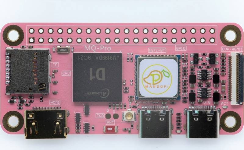 MangoPi MQ-Pro front view
The board is based on the Allwinner D1-H SoC, which was among the first widely available budget RISC-V CPUs on the market.
Here is the SoC description from the user manual:
D1-H is an advanced application processor designed for RISC-V Multi-Media decoding platform. It integrates a 64-bit XuanTie C906 RISC-V CPU and a HiFi4 DSP to provide the high-efficient computing power. D1-H supports full format decoding such as H.265, H.264, MPEG-1/2/4, JPEG, VC1, and so on. The independent encoder can encode in JPEG or MJPEG. Integrated multi ADCs/DACs and I2S/PCM/DMIC/OWA audio interfaces can work seamlessly with the CPU to accelerate multimedia algorithms and improve the user experience. D1-H supports RGB/LVDS/MIPI DSI/HDMI/CVBS OUT display output interfaces to meet the requirements of the different screen display. D1-H comes with extensive connectivity and interfaces, such as USB, SDIO, EMAC, TWI, UART, SPI, PWM, GPADC, LRADC, TPADC, IR TX&RX, and so on. Besides, D1-H can connect with other different peripherals like WiFi and BT via SDIO and UART.
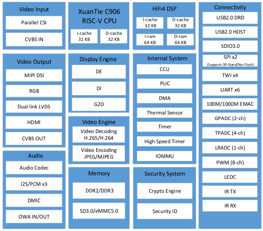 Allwinner D1-H SoC block diagram
The SoC integrates a single 64-bit XuanTie C906 RISC-V core, which is an open source RISC-V core design developed by Alibaba Group.
Core features from user manual:
- RV64IMAFDC instruction set architecture,
- 5-stage single-issue in-order execution pipeline,
- L1 instruction cache (I-Cache) and data cache (D-Cache) running on the Harvard architecture with a size of 32 KB and cache line size of 64 bytes,
- Sv39 memory management unit for virtual/physical address translation and memory management,
- AXI4.0 128-bit master interface supported,
- Core local interrupt (CLINT) controller and platform-level interrupt controller (PLIC) supported,
- RISC-V debug standard supported.
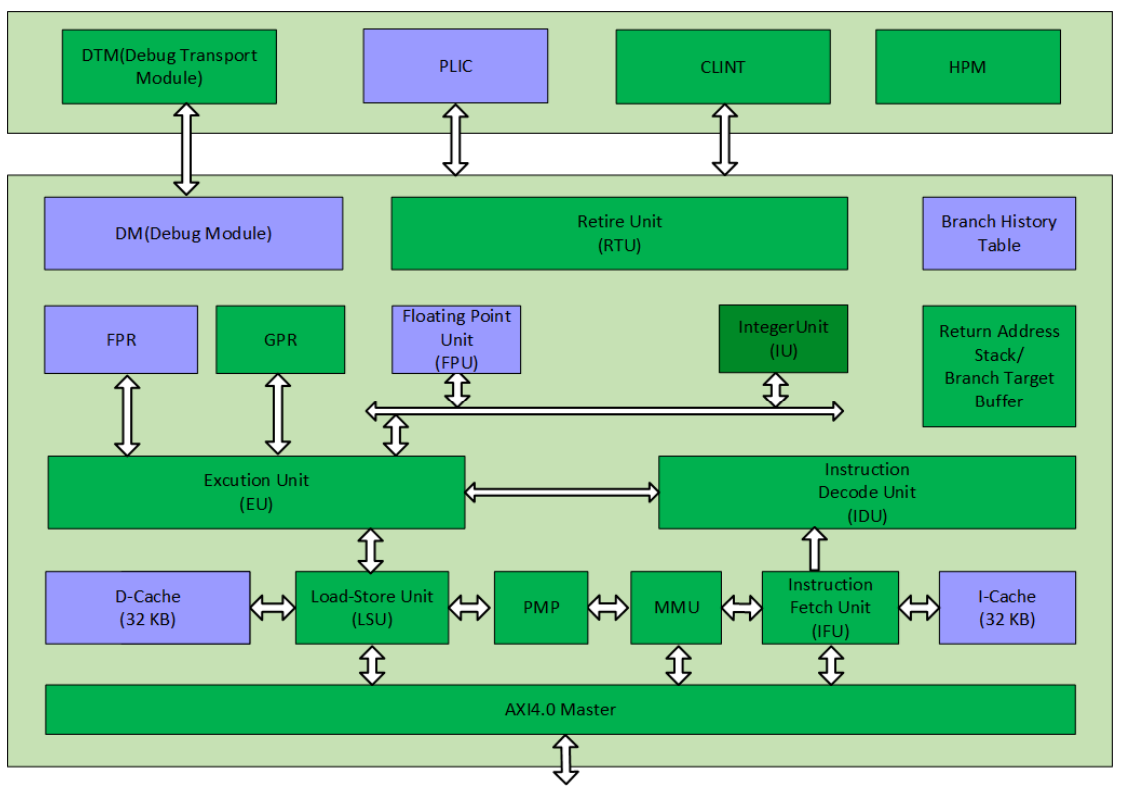 XuanTie C906 core structure
RV64IMAFDC instruction set means that we have a 64 bit (XLEN=64) RISC-V core with the following standard extensions:
- RV64I - Base Integer Instruction Set, 64-bit
- M - Standard Extension for Integer Multiplication and Division
- A - Standard Extension for Atomic Instructions
- F - Standard Extension for Single-Precision Floating-Point
- D - Standard Extension for Double-Precision Floating-Point
- C - Standard Extension for Compressed Instructions
Besides standard extensions, the core also implements custom instruction set extension called T-Head, which contains many additional instructions ranging from cache manipulation to half-precision floating point operations.
All in all, we will need the following reference documents to keep close by:
- MangoPi MQ-Pro Board Schematics
- Allwinner D1-H User manual
- XuanTie C906 User Manual
- RISC-V ISA Specifications
Software projects we will be using as a reference:
sun20i SPL: github.com/smaeul/sun20i_d1_spl. I didn't look into its origin, but this seems to be the original SPL (secondary program loader) boot code shipped with Tina Linux -- Linux distro developed by Allwinner that comes with the D1 demo board Nezha. At least some parts of the code look like they were shipped as object files and were reverse engineered later by the community (e.g. DRAM controller initialization code). It is now obsolete, as D1 and MangoPi support is now fully integrated into mainline U-Boot, but I find it more more convenient to use as a reference implementation because of its simplicity.
U-Boot: github.com/smaeul/u-boot. D1 support for mainline U-Boot.
Linux Kernel. Some relatable parts:
3. Blinking LED
Now that we have a basic grasp of the hardware, let's get to practice and write some code.
The board has a single user-controlled blue LED (DS2 in the schematics) connected to PD18 GPIO. Driving GPIO is trivial, so let's get straight to code.
_payload:
.equ GPIO_BASE, 0x02000000
.equ GPIO_PD_CFG2, 0x98
.equ GPIO_PD_DAT, 0xA0

/* Configure PD18 as output: GPIO_PD_CFG2[11:8] = 0b0001 */
li a0, GPIO_BASE + GPIO_PD_CFG2
lw a1, 0(a0)
li a2, 0xfffff0ff
and a1, a1, a2
ori a1, a1, 0x100
sw a1, 0(a0)

/* Invert PD18 state: ~GPIO_PD_DAT[18] */
li a0, GPIO_BASE + GPIO_PD_DAT
lw a1, 0(a0)
li a2, 1<<18

_blink:
xor a1, a1, a2
sw a1, 0(a0)

/* Sleep for 500ms and jump back */
li a3, 0
li a4,  0x40d9000
_delay:
addi a3, a3, 1
beq a3, a4, _blink
j _delay

_hang:
j _hang
Some notes on the code:
GPIO_BASEat0x02000000- MMIO GPIO registers block start address. The virtual memory is effectively disabled at this point, so we don't need to bother with memory mapping yet.GPIO_PD_CFG2atGPIO_BASE + 0x98- PD group configuration register 2 (pins 16 to 22). Each pin function is configured with a 4 bit value. The only relevant function for us is0b0001(output pin).GPIO_PD_DATatGPIO_BASE + 0xa0- PD group input/output state (one bit per pin).- The number of delay loop iterations can be calculated as
T * F / N, where T is the delay time in fractional seconds, F is the CPU core frequency and N is the number of cycles per one loop iteration. After the reset, the CPU is running at 408Mhz. We have 3 instructions per loop iteration and according to C906 user manual, each of these instructions has 1 cycle delay. Hence, 500ms delay requires0.5 * 408e6 / 3 = 0x40d9900iterations.
4. Building and running
Now, its not enough to just compile the code above and flash it to the SD card, as CPU BROM (boot ROM code) requires that specific header is present before the actual executable payload.
The only description of this header I found is in the comments of the original bootloader mentioned above. Here it is:
.text

.global _start

j _payload        /* jump over the metadata below to the actual payload */
.ascii "eGON.BT0" /* header marker (magic) */
.word 0x5f0a6c39  /* checksum initial value */
.word 0x00000000  /* payload size */
.word _payload - _start /* header size */
.word 0 /* public header size (we don't need one) */
.word 0 /* public header version */
.word 0 /* return address (dont care about this one) */
.word 0x20000 /* run address of the payload (SRAM A1) */
.word 0 /* boot cpu / eGON version (don't care) */
.dword 0 /* platform information (don't care) */

_payload:
/* ... our blinking LED program goes here ... */
The meaning of most fields should be clear from the comments, but some require further elaboration:
The checksum field holds a 32bit checksum of the payload. Here we only set the initial value, and will calculate the proper value with the
gencksumscript that we can pull from the original bootloader sources. Essentially, the checksum is calculated as a wrapping sum of all 32 bit words of the payload. You can find thegencksumscript sources in the Github repo for this series: github.com/alexeyden/os5/blob/p1-blinking-led/scripts/gencksum.The payload size field is the size of the payload in bytes. Again, it will be filled in by
gencksumscript.Run address field is set to point at the beginning of the 32K SRAM A1 area (
0x20000). This is where our code is going to be loaded and run by BROM. We don't use any stack or absolute addressing in our simple blinking LED program, and thus can stay oblivious to the actual run address, as long as we fit into the SRAM A1 region.
Finally, we are ready to compile the code above and flash it to the SD card. As for compiling, we will only need as and objcopy from the GNU RISC-V toolchain for now, as we're not compiling any Rust code yet. On Archlinux and Majaro, the toolchain can be easily installed with pacman -S riscv64-elf-binutils riscv64-elf-gcc.
For a program this simple, we also won't even need a linker script, so the only piece that's left is a convenience Makefile listed below.
FLASH_DEV?=/dev/sda

boot.img: boot.elf
	riscv64-elf-objcopy -O binary boot.elf boot.bin
	scripts/gencksum boot.bin boot.img
	rm -f boot.bin

boot.elf: boot.S
	riscv64-elf-as boot.S -o boot.elf

clean:
	rm -f boot.elf boot.img boot.img.S boot.elf.S

flash: boot.img
	[ -b $(FLASH_DEV) ]
	sudo dd if=boot.img of=$(FLASH_DEV) bs=8192 seek=1
	sync

boot.img.S: boot.img
	riscv64-elf-objdump -m riscv:rv64 -b binary -D boot.img > boot.img.S

boot.elf.S: boot.elf
	riscv64-elf-objdump -d boot.elf > boot.img.S

.PHONY: clean
A couple of notes on the makefile:
boot.imgis our primary build artifact and is produced by compiling theboot.Ssource into the ELF binary and then dumping all sections (just.textin our case) into the raw binary, stripping all metadata.gencksumscript then overwrites the checksum and length fields in place.We also have a couple of convenience targets that produce disassembled sources for the final binary (
boot.img.S) and the intermediate ELF file (boot.elf.S). They will come handy later for troubleshooting linker script issues and examining compiled Rust code.
All we have to do now is to build and flash the image with make flash FLASH_DEV=/dev/sdcard command, insert the SD card into the SBC and behold the results of our hard work.
5. What's next?
That's all for now! Next time we will be initializing the UART and finally running some Rust code.
Source code for the article is available on GitHub at: github.com/alexeyden/os5/tree/p1-blinking-led